Xscaping Limits Blog Series #4: Why AI Clusters Need Optics
In our last blog, we took a look at the “escape bandwidth” problem—the point at which data leaves the package and enters the data center fabric—incumbent to copper-based interconnects. That boundary is where AI system performance stops being determined by compute and starts being determined by efficient data movement and communication.
The problem is twofold. Legacy copper interconnects, which most current AI infrastructure is built around, are hitting fundamental scalability limits. Meanwhile, AI workloads and bandwidth demand are expanding far faster than our communication fabrics can sustainably support.
This begs the question, what comes next? The answer isn’t a faster version of copper, but a different physical carrier altogether: light.
As the name implies, silicon photonics uses photons, not electrons, as carriers of information across the fabric. Data is transmitted through optical waveguides, rather than electrical signals moving through resistive metal interconnects. This shifts data movement away from the physical constraints and loss inherent to copper, and more importantly, decouples bandwidth growth from those same restrictions.
Silicon photonics isn’t necessarily a cure-all scaling approach; its impact depends heavily on how much optical bandwidth is built into the fabric. Today, most systems scale bandwidth in two ways: by increasing per-channel data rates, or by adding more discrete optical links. Both approaches eventually run into a variety of system-level constraints in power, laser count, packaging complexity, thermal overhead, and more. At AI cluster scale, these effects become dominant factors in overall system efficiency.
This is where multi-wavelength transmission becomes a key differentiator. Using wavelength-division multiplexing (WDM), multiple independent data streams can coexist on a single optical path, each encoded on a different color of light (Figure 1). WDM allows bandwidth to scale both through additional physical interconnects, and through increased wavelength density on each interconnect. The challenge then becomes generating and managing those wavelengths efficiently, and at scale.
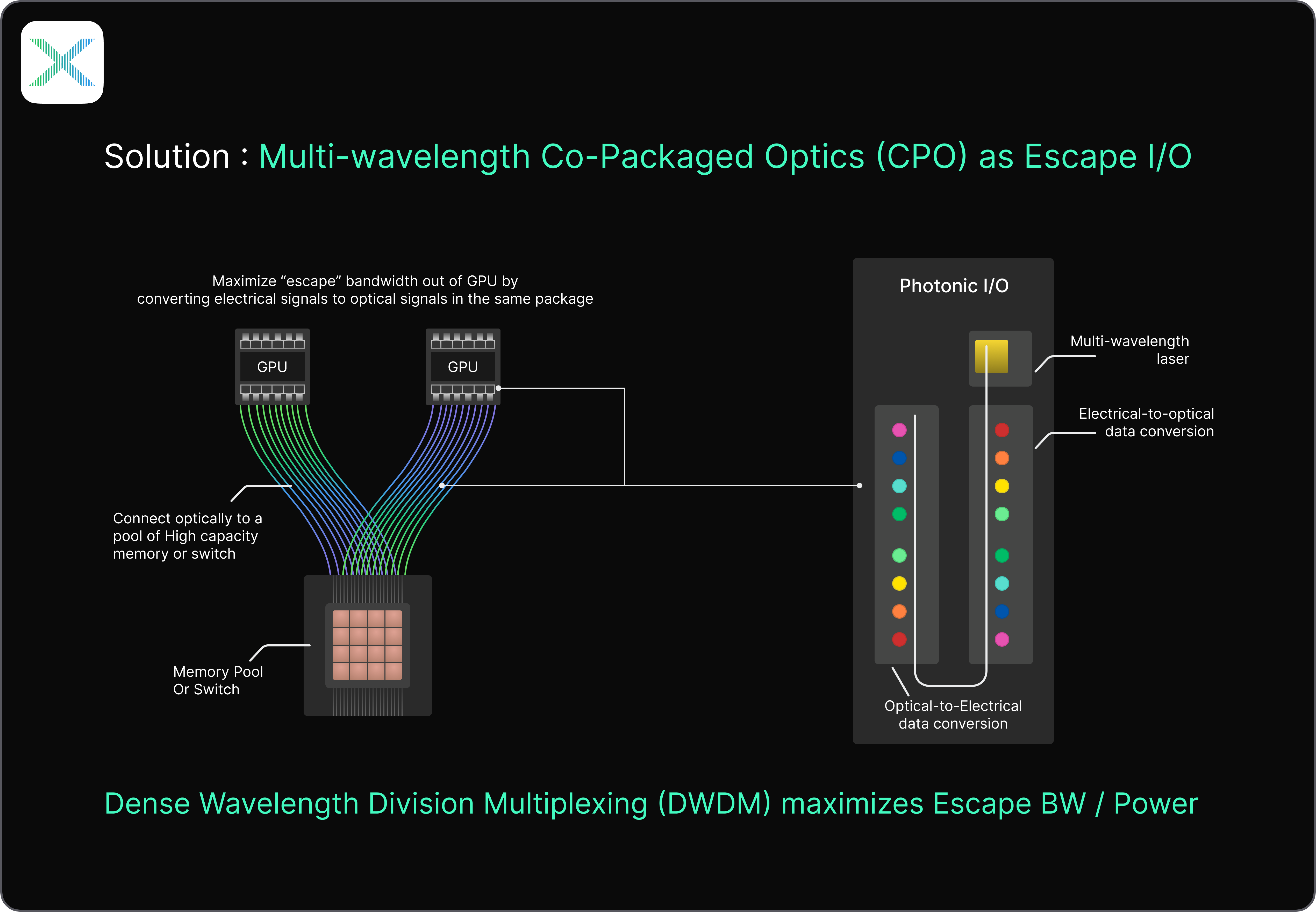
Recent advances in integrated photonics are accelerating progress in this direction. One promising approach is the use of optical frequency comb-based architectures, where multiple stable wavelengths are generated from a single on-chip source. Instead of relying on arrays of discrete lasers, each tuned and managed independently, these systems collapse multi-wavelength generation into a single coherent optical engine.
At a system level, this is a fundamentally different way of constructing bandwidth. Traditional data center fabrics build out communication capacity by packing in more physical resources, incurring a linear cost along the way. Early optical systems managed to improve per-channel data rates but inherited a similar scaling problem, as they still required more lasers and links with their own overhead. Multi-wavelength architectures introduce a new path to scaling, allowing multiple independent channels to coexist on the same device. This unlocks more communication capacity from the same physical footprint, improving overall data center and cluster efficiency.
Communication efficiency is becoming increasingly critical as AI workloads grow greater and more demanding. Training and inference for modern AI models—especially agentic systems and long-context reasoning—require immense amounts of data to move continuously across the fabric. As we’ve discussed in previous blogs, performance is already a function of data movement and communication efficiency rather than raw compute alone.
Viewed through that lens, silicon photonics is a lot more than a simple upgrade to copper-based fabrics, and will help reshape how AI systems are architected at scale. As communication bandwidth becomes less and less of a scarce resource, the way compute is organized across the data center can start to change. Systems today lean on measures like partitioned workloads to minimize communication wherever possible, to compensate for low off-chip bandwidth capabilities and the weak signal integrity of copper interconnects. But when the escape layer becomes significantly more efficient, those constraints loosen.
The system at large no longer needs to behave as a collection of loosely-coupled compute islands. Instead, it becomes possible to think of data center infrastructure as a more unified computational fabric, where workloads can be distributed more dynamically, and the system can spend less energy working around its own internal limitations.
In modern AI clusters, a meaningful portion of available compute is effectively idle at any given time, waiting for data to arrive across the fabric. As communication improves, that idle time decreases. There is a ceiling to how much more efficient it can get as a result of individual components getting faster; the real target is improving their synchronization across the fabric that connects them.
This, then, is the real inflection point of AI data center design. Peak FLOPs and high memory capacity are no longer an indicative metric for AI infrastructure’s value. Instead, communication efficiency is the true gating factor for whether additional compute actually translates into real performance gains.
Silicon photonics, especially multi-wavelength WDM architectures, directly target this layer of overall system cohesion by boosting escape bandwidth density and allowing more data to flow simultaneously. These technologies allow compute resources to be used as intended, instead of keeping them waiting for data to arrive. Practically, that means that adding more GPUs and accelerators actually can improve throughput, and won’t just tack on extra overhead cost with diminishing returns.
As optical interconnects become denser and more practical to deploy at scale, the gap between compute capability and real performance narrows. By breaking through the escape bandwidth barrier, or the “copper wall,” these fabrics let data move as fast as compute can handle it, opening up new levels of scale and complexity for AI workloads. The next generation of AI systems will be designed around communication at the speed of light, but optics alone does not solve the scaling problem.